- 您现在的位置:买卖IC网 > Sheet目录470 > MAX11014BGTM+T (Maxim Integrated)IC RF MESFET AMP 48-TQFN-EP
Automatic RF MESFET Amplifier
Drain-Current Controllers
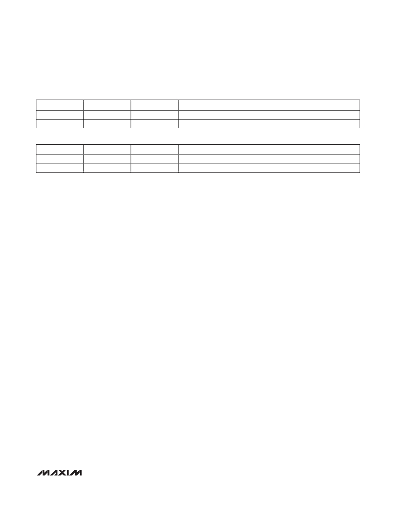
Table 14. VSET1 and VSET2 (Write)
BIT NAME
X
VSET11–VSET0
DATA BIT
D15–D12
D11–D0
RESET STATE
X
0000 0000 0000
FUNCTION
Don’t care.
VSET11 is the MSB and VSET0 is the LSB. Data format is straight binary.
Table 15. USRK1 and USRK2 (Write)
BIT NAME
X
K11–K0
DATA BIT
D15–D12
D11–D0
RESET STATE
X
N/A
FUNCTION
Don’t care.
K11 is the MSB and K0 is the LSB. Data format is straight binary.
Set the VALARM1 bit, D5, to 1 to enable ALARM func-
tionality for GATE1 voltage measurements. Set the
VWIN1 bit, D4, to 1 to monitor the GATE1 voltage with
the ALARM comparator in windowing mode. Set VWIN1
to 0 to monitor the GATE1 voltage with the ALARM com-
parator in hysteresis mode. Set the TALARM1 bit, D3, to
1 to enable ALARM functionality for channel 1 tempera-
ture measurements. Set the TWIN1 bit, D2, to 1 to moni-
tor the channel 1 temperature with the ALARM
comparator in windowing mode. Set TWIN1 to 0 to moni-
tor the channel 1 temperature with the ALARM compara-
tor in hysteresis mode. Set the IALARM1 bit, D1, to 1 to
enable ALARM functionality for channel 1 sense voltage
(RCS1+ to RCS1-) measurements. Set the IWIN1 bit, D0,
to 1 to monitor the channel 1 sense voltage with the
ALARM comparator in windowing mode. Set IWIN1 to 0
to monitor the channel 1 sense voltage with the ALARM
comparator in hysteresis mode.
VSET1 and VSET2 (Write)
Write to the channel 1/channel 2 V SET registers to set
the V SET(CODE) code in the V DAC(CODE) equations.
Writing to these registers triggers a V DAC(CODE) calcu-
lation. That code is then loaded into either the channel
1/channel 2 DAC input register or channel 1/channel 2
DAC input and output register, depending on the state
of the LDAC1/LDAC2 bits in the software configuration
register. Set the command byte to 40h to write to the
channel 1 V SET register. Set the command byte to 42h
to write to the channel 2 V SET register. See Table 14.
Bits D15–D12 are don’t care. Bits D11–D0 contain the
straight binary data.
USRK1 and USRK2 (Write)
Write to the channel 1/channel 2 K parameter registers
to set the LUT K [K] code in the V DAC(CODE) equation.
The K parameter register value is loaded into the
V DAC(CODE) equation when the KSRC_-2/KSRC_-1/
KSRC_-0 bits in the software configuration register are
set to 010, 101, 110, or 111. See Table 11b. Use the K
parameter as an index to the KLUT or as a multiplier for
the V DAC(CODE) equation in place of V SET(CODE) by
writing to the software configuration register. See Table
11. Set the command byte to 44h to write to the channel
1 K parameter register. Set the command byte to 46h to
write to the channel 2 K parameter register. See Table
15. Bits D15–D12 are don’t care. Bits D11–D0 contain
the straight binary data.
IPDAC1 and IPDAC2 (Write)
Write to the channel 1/channel 2 DAC input registers to
load the DAC code and bypass a V DAC(CODE) calcula-
tion. Transfer the code written to the DAC input registers
to the channel 1/channel 2 DAC output registers by set-
ting the corresponding DACCH_ bit high in the software
load DAC register. Set the command byte to 48h and
4Ch, respectively, to write to the channel 1/channel 2
DAC input registers. See Table 16. Bits D15–D12 are
don’t care. Bits D11–D0 contain the straight binary data.
Writing to these registers overwrites any previous val-
ues loaded from the V DAC(CODE) calculation.
______________________________________________________________________________________
43
发布紧急采购,3分钟左右您将得到回复。
相关PDF资料
MAX12000ETB+T
IC AMP GPS FRONT 1575MHZ 10TDFN
MAX12005ETM+T
IC SATELLITE IF SWITCH 48-TQFN
MAX1385BUTM+
IC RF LDMOS BIAS CNTRLR 48-TQFN
MAX1470EUI+T
IC RECEIVER 315MHZ 28-TSSOP
MAX1470EVKIT-315
EVAL KIT FOR MAX1470 315MHZ
MAX1471EVKIT-315
EVAL KIT FOR MAX1471 315MHZ
MAX1472EVKIT-433#
EVAL KIT MAX1472
MAX1473EVKIT-433
EVAL KIT MAX1473
相关代理商/技术参数
MAX11014EVKIT+
制造商:Maxim Integrated Products 功能描述:EVALUATION KIT FOR THE MAX11014 - Bulk
MAX11015
功能描述:射频放大器
RoHS:否 制造商:Skyworks Solutions, Inc. 类型:Low Noise Amplifier 工作频率:2.3 GHz to 2.8 GHz P1dB:18.5 dBm 输出截获点:37.5 dBm 功率增益类型:32 dB 噪声系数:0.85 dB 工作电源电压:5 V 电源电流:125 mA 测试频率:2.6 GHz 最大工作温度:+ 85 C 安装风格:SMD/SMT 封装 / 箱体:QFN-16 封装:Reel
MAX11015BGTM
制造商:MAXIM 制造商全称:Maxim Integrated Products 功能描述:Automatic RF MESFET Amplifier Drain-Current Controllers
MAX11015BGTM+
制造商:MAXIM 制造商全称:Maxim Integrated Products 功能描述:Automatic RF MESFET Amplifier Drain-Current Controllers
MAX11017
功能描述:模数转换器 - ADC
RoHS:否 制造商:Texas Instruments 通道数量:2 结构:Sigma-Delta 转换速率:125 SPs to 8 KSPs 分辨率:24 bit 输入类型:Differential 信噪比:107 dB 接口类型:SPI 工作电源电压:1.7 V to 3.6 V, 2.7 V to 5.25 V 最大工作温度:+ 85 C 安装风格:SMD/SMT 封装 / 箱体:VQFN-32
MAX11017ATL+
功能描述:模数转换器 - ADC
RoHS:否 制造商:Texas Instruments 通道数量:2 结构:Sigma-Delta 转换速率:125 SPs to 8 KSPs 分辨率:24 bit 输入类型:Differential 信噪比:107 dB 接口类型:SPI 工作电源电压:1.7 V to 3.6 V, 2.7 V to 5.25 V 最大工作温度:+ 85 C 安装风格:SMD/SMT 封装 / 箱体:VQFN-32
MAX11017ETL+
功能描述:模数转换器 - ADC
RoHS:否 制造商:Texas Instruments 通道数量:2 结构:Sigma-Delta 转换速率:125 SPs to 8 KSPs 分辨率:24 bit 输入类型:Differential 信噪比:107 dB 接口类型:SPI 工作电源电压:1.7 V to 3.6 V, 2.7 V to 5.25 V 最大工作温度:+ 85 C 安装风格:SMD/SMT 封装 / 箱体:VQFN-32
MAX11019
功能描述:模数转换器 - ADC
RoHS:否 制造商:Texas Instruments 通道数量:2 结构:Sigma-Delta 转换速率:125 SPs to 8 KSPs 分辨率:24 bit 输入类型:Differential 信噪比:107 dB 接口类型:SPI 工作电源电压:1.7 V to 3.6 V, 2.7 V to 5.25 V 最大工作温度:+ 85 C 安装风格:SMD/SMT 封装 / 箱体:VQFN-32
